Reverse Engineering my HP Prime’s LCD (and upgrading it with an IPS panel)
You may have seen my previous blog post about adding a USB-C port to my favorite calculator, the HP Prime. In that article, I mentioned that some day, I hoped to perform further modifications, beginning with finding a replacement for the calculator’s low quality touchscreen. This article summarizes the work I have done so far towards reaching that goal.
The stock HP Prime LCD panel (320×240) has poor viewing angles and low contrast. Additionally, it suffers from a relatively dim backlight in comparison to more modern electronic gadgets. In light of these blights on an otherwise solid product, I set out to find a superior alternative LCD panel and figure out how to cram it into the HP Prime. This was the entrance into a much deeper technical rabbit hole.
My ultimate goal was to install a more modern LCD panel in the place of the original LCD. Modern IPS LCD panels have better contrast ratios and brighter backlights. Perplexingly, despite HP having the original LCD panel custom-made, the design is flawed such that the LCD is actually mounted in an upside-down configuration from its optimal viewing angle. As a result, colors and contrast appear seriously washed-out at most everyday viewing angles, and the calculator’s dark mode, which should be a headline feature, ends up being more of an unusable afterthought.
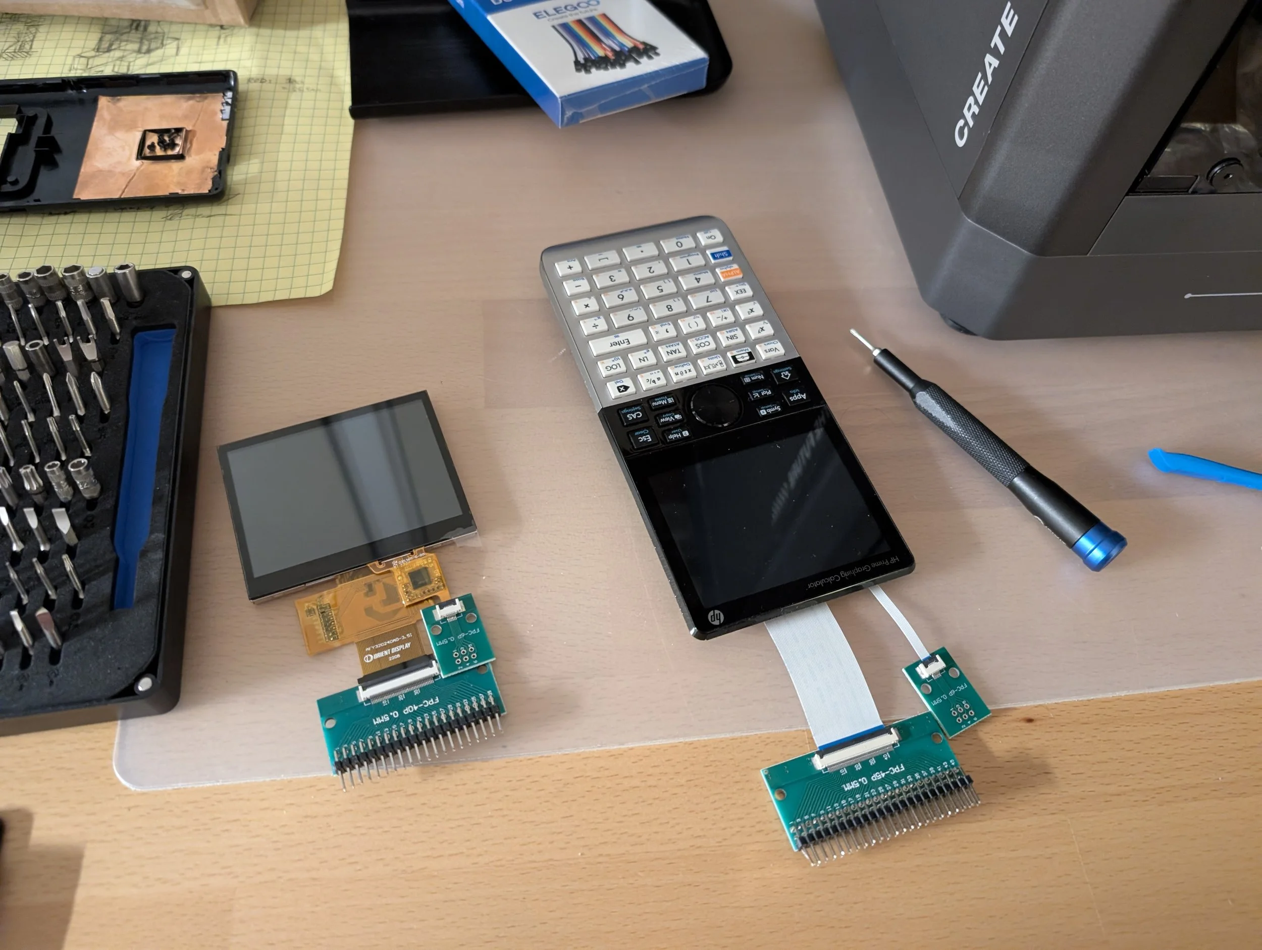
I used flat flex breakouts to wire up my prototype
I knew from prior experience in tearing down the HP Prime that there was an unlabeled 45 pin ribbon cable connecting between the LCD panel and the main motherboard. This cable reminded me of a Hackaday article I had read about parallel RGB LCD protocols, which I assumed the HP was using as well. But doing some further research, and hoping to find a drop-in-replacement LCD panel, I discovered that most common parallel LCDs use 40 pin LCD cables, not 45 pin cables. So something funny was going on here…
This pin count discrepancy wasn’t immediately an issue, especially if I could determine the stock pinout and design a simple passive interposer board. So I researched the stock LCD panel, typing every label, model number, and serial number associated with the panel into Google, but I was unable to find an exact match for the original panel. Eventually I realized the original LCD glass touch digitizer has a rounded front and HP labeling printed on it, so it should have been more obvious that this was a custom part to me from the beginning.
Undeterred, I set out to reverse-engineer the pinout of the stock LCD in order to find a way to adapt a more common commercial LCD panel to fit the signals coming out of the motherboard. I needed to be able to see signals going into the screen while the original LCD panel was still connected. My first step was to create a spreadsheet with 45 rows (one row per pin,) and then probe each LCD signal using an oscilloscope. As the pin pitch on the original LCD ZIF FFC connector was extremely fine, it wasn’t possible for me to safely measure these signals with my chunky oscilloscope probe. As a workaround, I decided to build a custom pass-through sniffer cable that would break out the signals from the calculator to larger test pads that I could easily probe. I used a combination of FFC breakout boards and FFC extension cables to cobble this together.
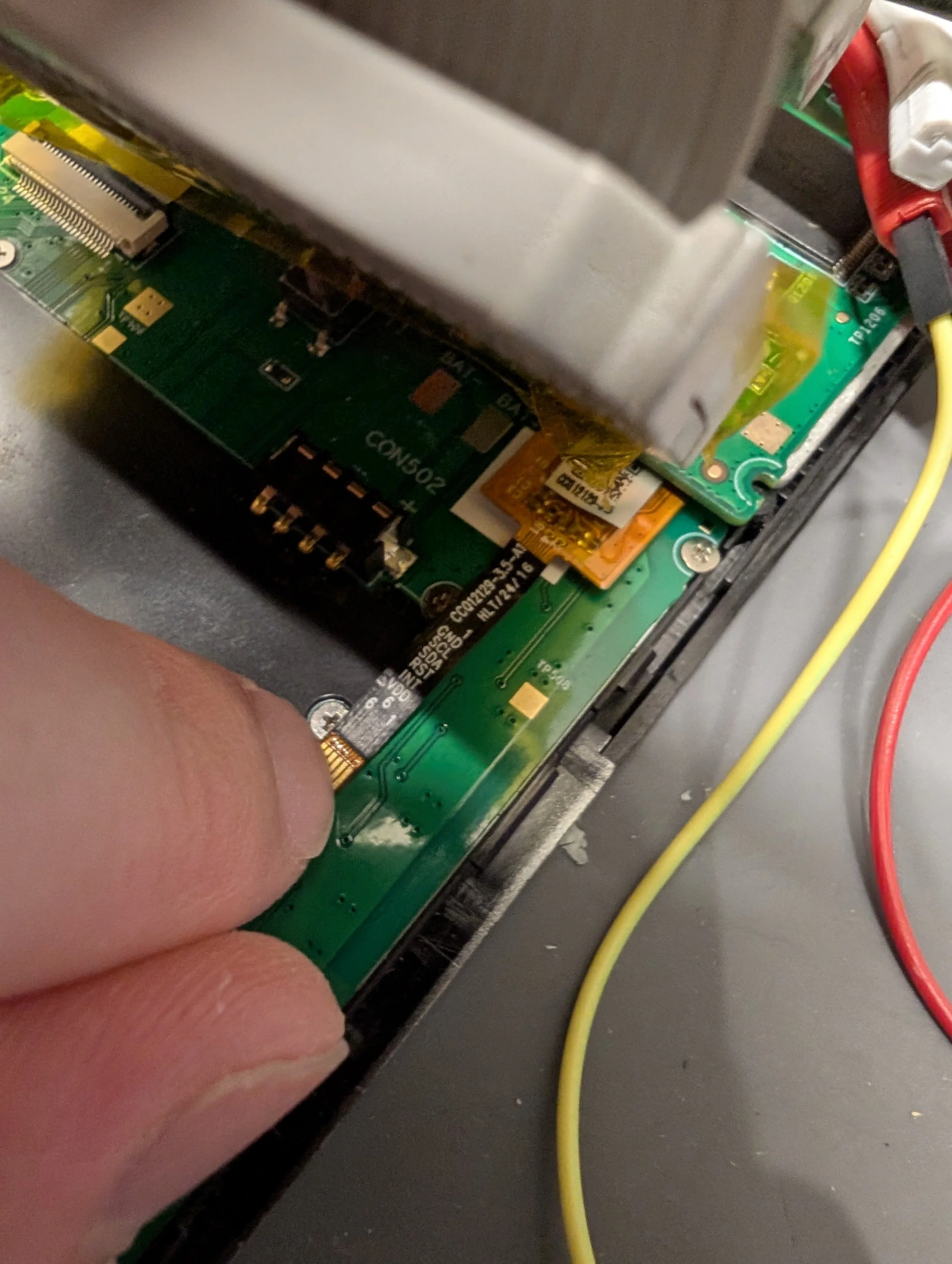
The labeled I2C Touch Digitizer Flex Cable
Measuring the original cables within the calculator, I found that there was a 45 pin 0.5mm pitch cable connecting the LCD panel to the calculator motherboard and a separate 6 pin 0.5mm pitch FFC cable connecting the touchscreen’s digitizer layer to the motherboard. The presence of a separate 6 pin touchscreen specific FFC cable meant that the 5 unaccounted-for pins on the 45 pin video cable were probably NOT meant for transmitting touchscreen data. Thankfully, the 6 pin digitizer cable was labeled with a handy pinout indicating that it used a common I2C protocol.
Building the breakout board was where I ran into my next hurdle, learning the difference between type A and type B flat flex cables. While in hindsight it might be obvious, I hadn’t realized when ordering the parts for my project that some FFC cables put the electrical contacts on the same physical side of the cable, while others place the contacts on opposite faces at either end of the cable. Because I accidentally ordered the wrong variety of the cable, I quickly realized that the signals weren’t getting mapped where they needed to go. Using a combination of an old frankensteined SCSI cable where I flipped all of the wires around, and manually soldering to the contacts inside an FFC cable under a microscope, I was eventually able to cobble together a suitable test jig. I searched extensively for a commercial product that did what I needed before going to these extreme lengths, but I couldn’t find anything easily available, and I didn’t feel like making a custom PCB for this phase of the investigatory process.
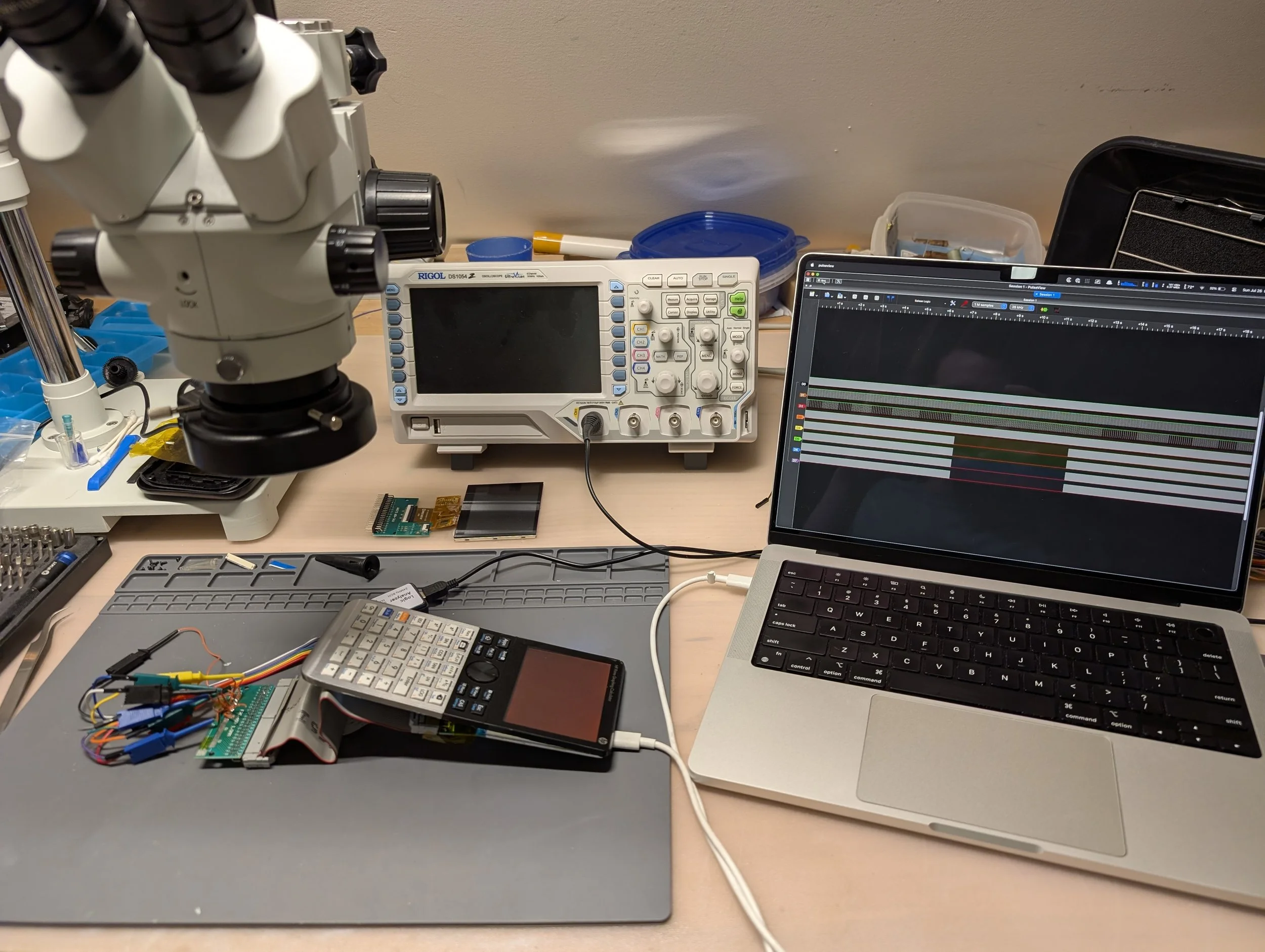
Logic Analyzer Capture with Sigrok Pulseview
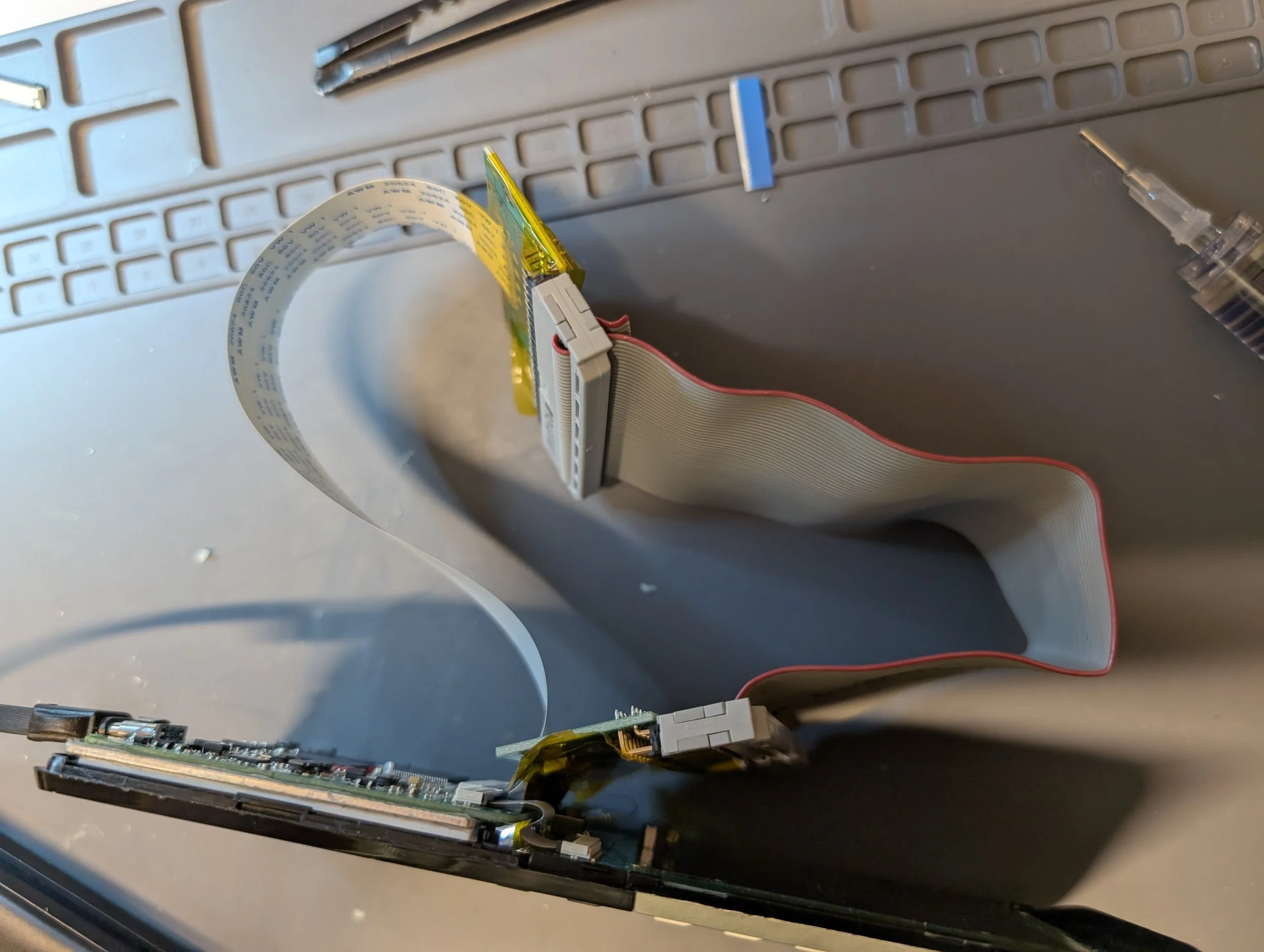
FFC-SCSI Inline Sniffing Abomination
My initial oscilloscope probing left me with a list of clock speeds, waveform shapes, and voltages. I used this preliminary information to select a series of test points to which I would then connect a $5 Aliexpress 24Mhz logic analyzer. Using Sigrok’s Pulseview software and 8 logic channels at a time, I was able to take some logic analyzer captures of the most promising looking signals going into the LCD panel. I wrote a quick and dirty HP Prime program to display solid-color RGB test patterns on the HP Prime LCD panel, and I used this as a technique to attempt and determine how color information was encoded in the original LCD’s protocol.
Armed with the power of agentic AI, in this case Claude Opus 5, I was able to write some python programs to perform analysis on the signals captured with my logic analyzer. Impressively, AI analysis of the binary data revealed that the signaling was not in fact parallel RGB at all, but rather a form of serial RGB. It was around this time that I stumbled upon Wenting Zhang’s fantastic HP Prime reverse engineering work from several years ago. Helpfully, Wenting noted that the HP Prime LCD uses an ILI9322B style serial RGB protocol. So with that major revelation out of the way, I realized I would either need my new LCD panel to be Serial RGB compatible, or I would need to adapt serial RGB to parallel RGB. I opted for the latter approach, which proved to be an interesting challenge.
With signals flying around the data bus at over 13MHz, I realized that bit-banging things using a microcontroller like the Raspberry Pi Pico to perform this style of conversion would be dicey (although potentially doable with the Pico’s PIO). So instead, I hopped over to Amazon, and I ordered the Sipeed Tang Nano 20k, an (comparatively) inexpensive $38 FPGA devboard. With an FPGA, I could build a custom solution to adapt the signals from serial to parallel in hardware, rather than in software, which meant that I could perform the necessary translations at a much higher speed.
I chose this specific FPGA for a few reasons:
Cheap for an FPGA ($38)
ZIF socket to accept a parallel RGB LCD (to which I intended to connect my upgraded LCD panel)
Lots of IO for sniffing the signals from the original LCD panel
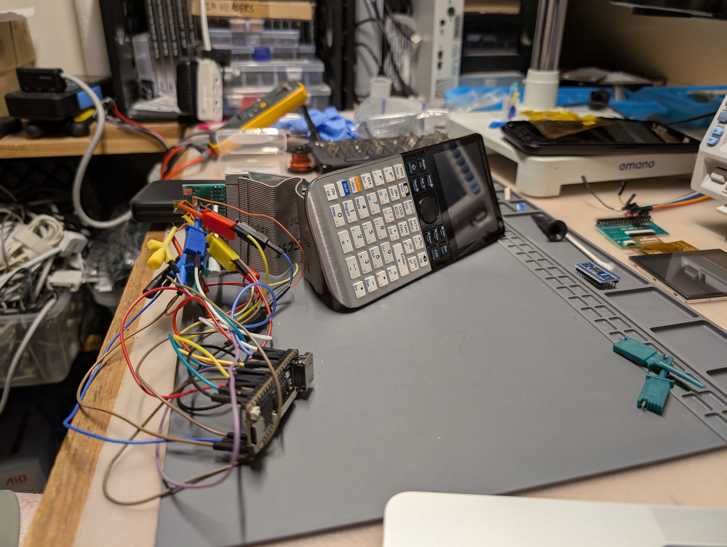
Connecting the Tang Nano 20k to the HP Prime
Despite having two semesters of FPGA programming under my belt, I wasn’t too keen on hand-writing a Verilog solution to this serial-to-parallel conversion problem. So instead, I opted for a different approach, leveraging the power of agentic AI for FPGA hardware development. In the process, I learned a lot of new techniques to get the most out of AI for a hardware and FPGA project of fairly high complexity. As of right now in 2026, AI and large language models aren’t commonly used to write code for FGPAs, which are essentially software-defined hardware, rather than microprocessors. This is in part because something like Verilog is considered more of a “hardware description language” rather than a programming language.
Starting out with the Gowin FPGA toolchain provided with the Tang Nano, I quickly shifted gears into using a custom developed toolchain that made working with the FPGA far more efficient and leverages common open-source FPGA tools.
I started out with the following plan in mind:
Implement an FPGA hardware UART so I could interface the FPGA with my MacBook and stream data off of it through the serial port
Turn the FPGA into a rudimentary logic analyzer with far greater capacity and more IO than the $5 Aliexpress gadget I had been using
Capture the serial RGB signals from the original LCD
Write some python scripts to decode the captured LCD signals on my laptop and display screen captures —this would prove I had a functional grasp of the original LCD’s protocol
Drive a new parallel RGB LCD panel with the FGPA (show some basic test patterns)
Stream the captured data from the HP Prime into the new parallel RGB LCD live (an Orient Display AFY320240A0-3.5INTH-C2)
Capture and convert the data from the touch digitizer panel on the new LCD to be compatible with the HP Prime (although both were I2C, they use different addresses)
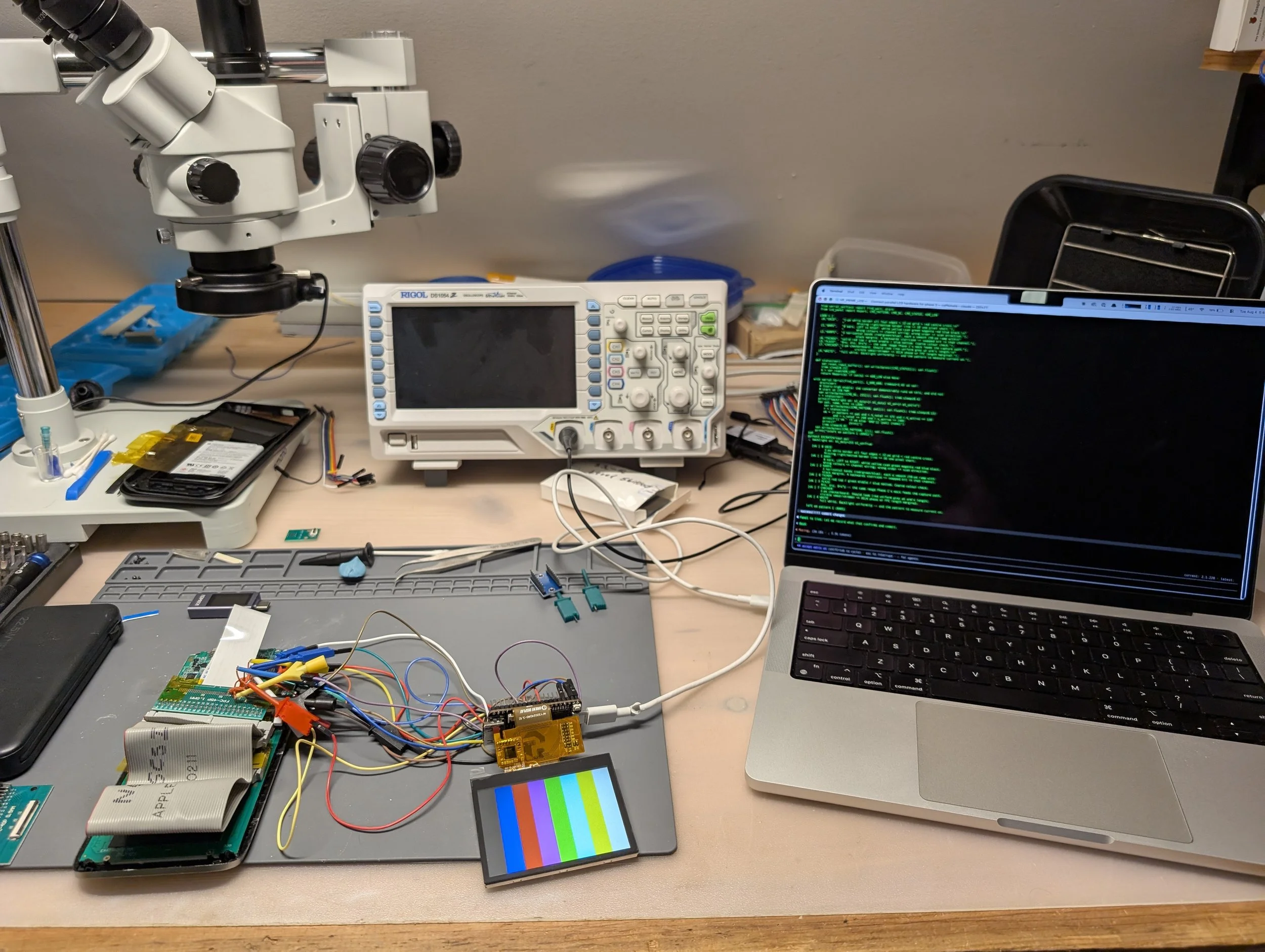
With Claude Opus 5, I was able to experimentally develop a toolchain that would let me take an agentic development approach. (Disclaimer, while I wrote oodles of Verilog with the aid of AI, the article you are reading right now was entirely hand-written by me, a genuine human.) But you probably don’t want to read yet another article about AI, so I’ll keep the rest of my thoughts on this brief for now.
The specifics of the toolchain are documented in my GitHub repo linked here: https://github.com/davidg5678/HP-Prime-IPS-LCD-Mod-FPGA
I’m primarily relying on Verilator and Icarus for simulations, and using Gowin’s proprietary IDE shell for synthesis. I found that this specific combination of tools offered the best tradeoffs as far as speed and producing useable/relatively bug-free Verilog results went.
I specifically instructed the AI to create mock hardware to test each phase of the project against before eventually switching to real hardware. Using FPGAs meant that I could internally multiplex the signals within the IC and create internal mock hardware replicas of the expected external hardware. Letting AI take a preliminary stab at mock hardware leveraging this agentic approach meant that many major bugs were caught without the need for significant human intervention. Of course, I supervised the process the entire time, dictating the approach, methodology, goals, tools, priorities, etc.
I really think the potential for AI-assisted FPGA work is absolutely brilliant, and I expect to see more projects done with an agentic approach like mine become more common in the near future. I have some major criticisms of Claude Code with Opus 5 as well however. I felt that it was overeager to forge ahead without stopping to ask me for critical feedback or ask clarifying questions . It often added complexity to the project that I didn’t ask it to, and it sometimes got stuck and tried troubleshooting with ever more complex techniques, rather than just pausing and letting me intervene. I eventually got fed up and addressed many of these issues with a custom system prompt. I also set up Claude to keep a running log of its progress, architecture, and goals so that I could start new sessions with completely fresh context windows on an as-needed basis.
Working alongside the AI, I steered it away from some of its more questionable design choices, like a determination to stream relatively high-bandwidth live video over the serial UART, or an insistence on rewriting macOS’s serial drivers because the FPGA was unplugged and it didn’t think to ask me to check.
Eventually, I reached a major milestone: I captured the signals from the original LCD with the FPGA and decoded them on my laptop. This left me with a pixel-perfect screen capture! I needed to access the Tang Nano’s RAM and use it as a buffer for this, as there wasn’t quite enough headroom with the original architecture I settled upon. Ultimately, this addition of RAM buffering to the project wasn’t an issue.
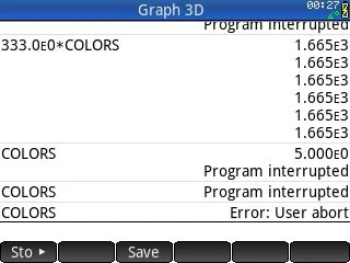
The first successful hardware-level screenshot taken on an HP Prime with my FPGA setup
Attaching a fancy new 900 nit IPS LCD panel to the ZIF connector on the Tang Nano, I was eventually able to drive it with the FPGA and display some test patterns. I spent an embarrassingly long amount of time dealing with the same FFC Type A vs Type B problem a second time before eventually learning my lesson to quadruple-check physical pin locations.
From this point, it wasn’t too far a leap to get a live stream of video from the HP Prime motherboard to display on the upgraded LCD panel. Text is crystal clear, lag is unnoticeable, and colors look correct to my eyes. The viewing angles and contrast levels of the upgraded panel are a serious improvement, and dark mode is perfectly usable now.
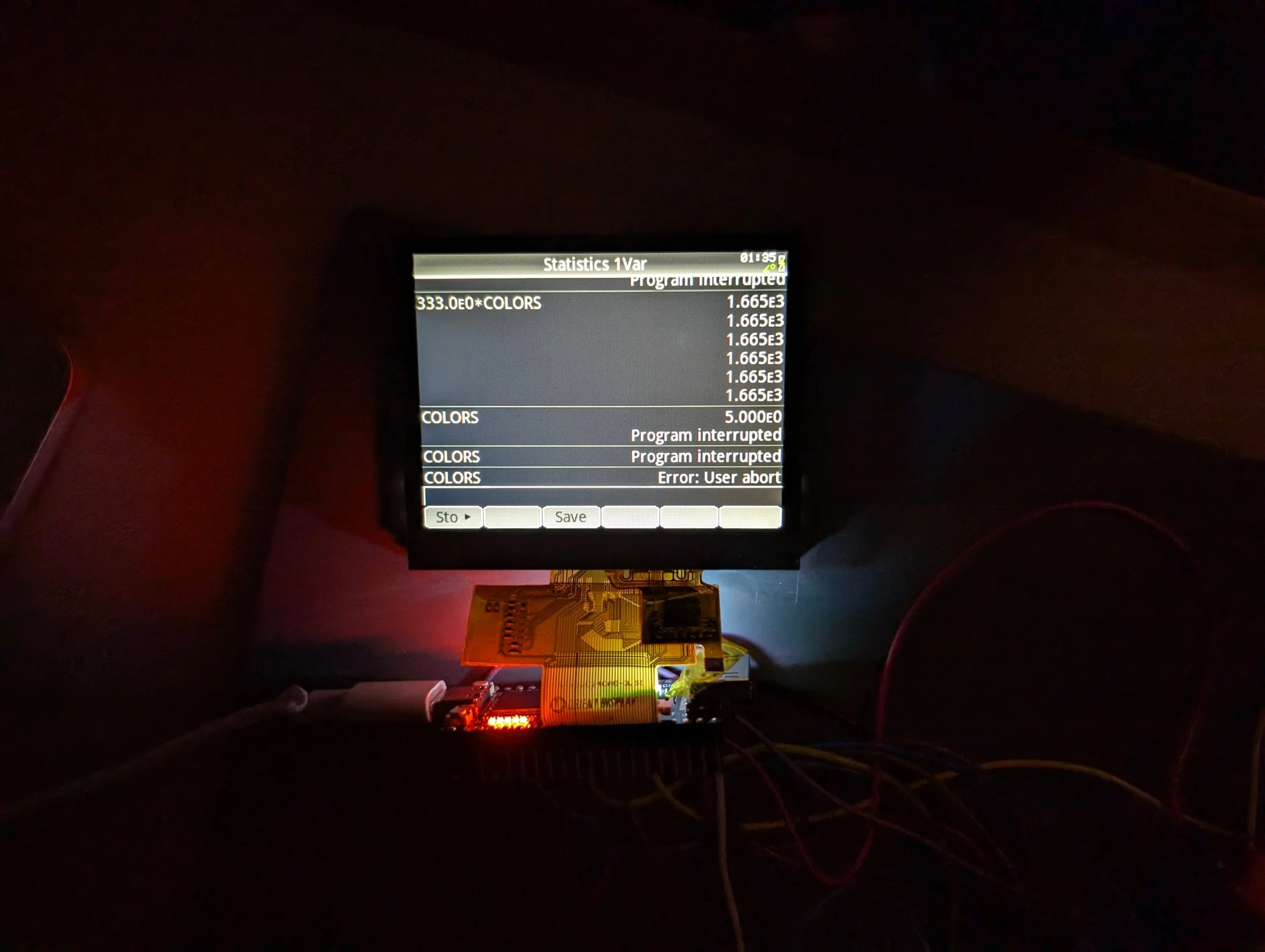
Excitingly, I found that I didn’t need to keep the stock LCD panel connected at the same time as the upgraded LCD panel to capture the video signals I needed. In the end, I used nearly every easily accessible IO pin on the Tang Nano 20k devboard. I got really lucky that it was just enough to meet the needs of my project.
So what work remains to be done? I need to cram this spaghetti mess of wires back into the chassis of the calculator and make it power-efficient and portable again. Arguably the hardest work is complete. I’m envisioning making a custom interposer PCB with the FPGA onboard. Strangely enough, while the Tang Nano FPGA devboard I bought was $38, as of the time of writing, Mouser Electronics quotes nearly $70 for the IC alone! If I can’t manage to find an alternative and much cheaper FPGA supplier, I’ll either have to transplant the FPGA IC off of the devboard, or I’ll fabricate a thicker 3D-printed back panel for the HP prime with enough wiggle room to safely accommodate the entire devboard.
Furthermore, I’d like to take some power efficiency measurements to see how this mod impacts the HP’s already poor battery life. But I’ll use the larger back panel as an opportunity to cram in a larger battery, better utilizing the extra space.
All of this work and more is open for further investigation. But for the time being, a new semester has begun, and I’m out of time to work on this project for a while.
All of my work so far is open source and available on GitHub: https://github.com/davidg5678/HP-Prime-IPS-LCD-Mod-FPGA
If anyone is eager to spin up some PCBs from the pinouts I’ve placed on GitHub and collaborate with me on this, don’t hesitate to reach out! Otherwise, I hope to continue this project someday (hopefully soon) in the future.